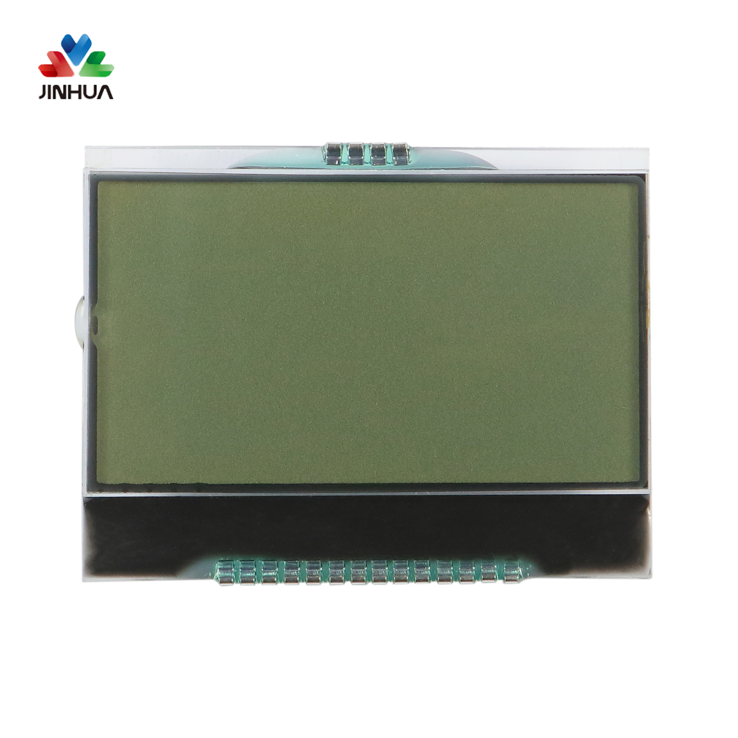
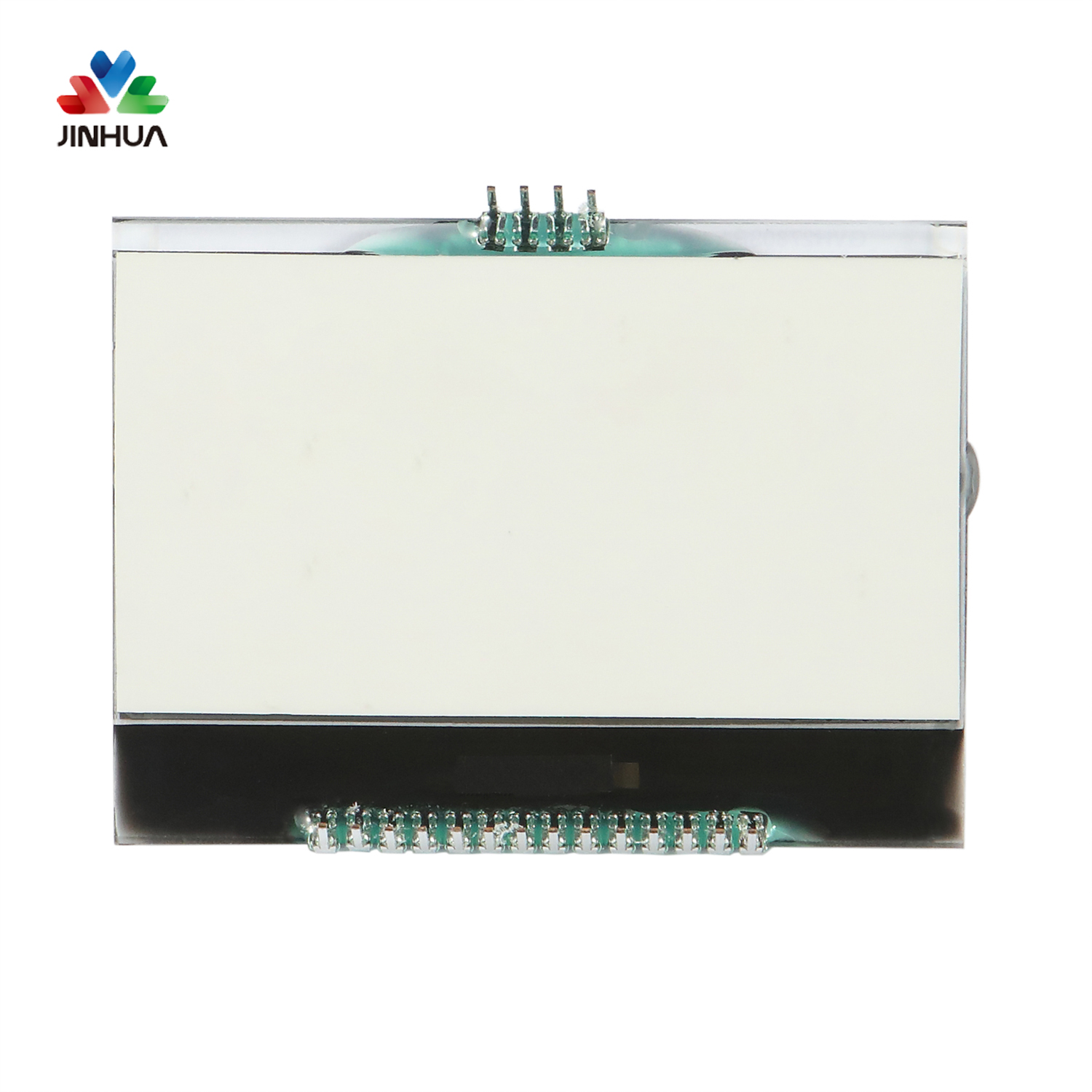
Chip-On-Glass (COG) is a flip-chip bonding method for directly connecting bare integrated circuits (ICs) to glass substrates by using an anisotropic conductive film (ACF). The pitch (footprint) of the IC bumps can be scaled down according to customer requirements (contact pitch of the glass substrate). This method reduces the assembly area to the highest possible packaging density, which is particularly important for applications where space saving is critical. Since the integrated flexible PCB is no longer needed, the driver chip can be installed cost-effectively. The IC is directly attached to the glass substrate and is suitable for processing high-speed or high-frequency signals.
COG technology is one of the high-tech mounting methods using gold bumps or flip chip ICs and is implemented in most compact applications. Chip-On-Glass integrated circuits were first introduced by Epson. In flip-chip mounting, the IC chip is not packaged, but is directly mounted on the PCB as a bare chip. Since there is no package, the IC installation footprint and the required PCB size can be minimized. This technology reduces the installation area and is more suitable for processing high-speed or high-frequency signals.
COG is mainly used for source driver ICs in TFT display module technology, and they are used for LCD, plasma, electronic ink, mini OLED screen or 3D technology. This is essential for consumer electronics products (such as laptops, tablets, cameras, or mobile phones) that require small size and lightweight components.
Advantages:
1. The size is very economical. The Chip-On-Glass LCD module can be as thin as 2 mm.
2. More cost-effective than COB, especially in graphic LCD modules, because it reduces the number of ICs.
3. Due to TAB's weakness in the bond field, it is more reliable than TAB.
Disadvantages:
1. COG can only be used for certain resolution levels where the lines are not too fine. At very fine pitches, COG becomes difficult to test, TAB will be the preferred method.
2. If the designer must integrate a keyboard or indicator around the display, it may be more cost-effective to use TAB or COB.
3. Due to the area where the circuit is located, the active area is not centered within the contour but offset.


 English
 Deutsch
 русский
 español
 العربية


 IPv6 network supported